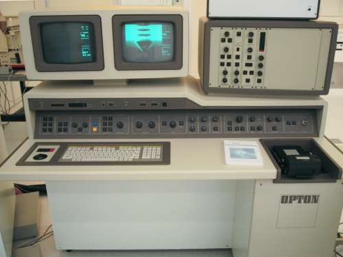
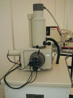
Zeiss/Opton DSM-950 Scanning Electron Microscope
A scanning electron microscope scans a tightly focused electron beam across the surface of an electrically conductive sample. Secondary and back-scattered electrons are emanated where the e-beam strikes the sample surface. By detecting this electron flux, an image of the sample surface is created, at magnifications up to 200000 times.
The SEM is used for measuring and imaging submicrometer-scale structures that are too small for optical microscopy, and 3-dimensional structures that benefit from the greater depth-of-field of the SEM. The system has also been modified for use as an electron-beam lithography tool, and can be used for electron-beam induced current (EBIC) analysis.
A Balzers SCD-050 sputter is available for gold-plating non-conductive samples prior to SEM imaging.